The Essentials of FPGAs with Verilog
FPGAs (field programmable gate arrays) were first developed in the 1980s and have since been used in telecommunications, high frequency trading, and guidance missile systems. They are especially useful for applications that require high speed and/or low energy digital electronics; in this article, I’ll try to give a concise introduction to the process of programming them with Verilog.
What are FPGAs?
To simplify things, you can think of an FPGA as a ‘chip’ that contains a whole lot of logic gates (read up on those if you don’t know what they are) and registers that can be connected in any which way to create a digital circuit. If you didn’t already know, all computers and processors are made up of logic gates and registers, so yes, you could build a computer processor with an FPGA.
Actually though, FPGAs are mostly made up of LUTs (look up tables) and flip-flops. Flip-flops are used to store bits of data (i.e. a 0 or a 1), and a set of flip flops together can form a register capable of storing large numbers. LUTs are used to perform logic operations, taking in an input and outputting some corresponding pre-determined value. A LUT is like a logic gate but with many more input and output states.
You can program FPGAs using a HDL (hardware description language) such as Verilog. A HDL is not a programming language like C or Python, since languages like these are translated into machine instructions and fed through a processor. Instead, a HDL describes the structure of a processor itself, line-by-line.
Why use FPGAs when we have easy-to-use computers and microcontrollers already?
Because FPGAs are optimised for a specific process, they are faster and more power efficient than off the shelf processors when used correctly. To improve speed and power efficiency even further you can use PCBs (printed circuit boards), however PCBs are obviously not programmable. FPGAs are often used in the intermediate stage of designing a digital circuit, used to optimise a system and iron out logical errors before an equivalent unmodifiable circuit is manufactured.
What is Verilog and how do I use it?
Verilog is a popular HDL widely used in industry. As mentioned above, a HDL like Verilog is used to describe the structure and behaviour of a digital circuit to be implemented on an FPGA.
A popular way to program FPGAs is by using a program called Vivado. Vivado can also simulate the behaviour of an FPGA, making it possible to troubleshoot logical errors before implementing your HDL on physical hardware. When simulating a circuit, you will also need to write a testbench which describes the simulated inputs.
Part 1 — Verilog Basics
Let’s start with a rudimentary example: a 1-bit NOT gate. As we know, a NOT gate simply inverts a signal.

First, we need to write a module. Modules are like functions in a programming language; they’re used to modulate our HDL code into simple parts for easier debugging. Given the trivial nature of our example, we’ll only need one module:
module invert_bit (
  input i,
  output o
  );

  o <= ~i; // Assigns o to the inverse of i

endmodule
At the top of the module, we declare the module name and inputs/outputs. These inputs/outputs are like pins on an IC. Then we describe the logic, where we simply assign the output as the inverse (~) of the input. We end every module with the endmodule keyword.
The ‘~’ is a bitwise operator. Here is the complete list of Verilog bitwise operators:
- ~ = NOT
- & = AND
- | = OR
- ^ = XOR
Part 2 — Mutliple Inputs/Outputs
In the previous example, we used a single 1-bit input and a single 1-bit output. We can have multiple inputs and multiple outputs. We can also group together inputs and outputs to simplify things where larger numbers need to be operated on. In case you need some quick revision, since we’re using digital circuits, each wire/register can be either a 1 or a 0. If we have 2 registers/wires, we can represent a 0, 1, 2, or 3. This can be generalised in that for n bits (wires/registers) we can represent the numbers between 0 and (2^n)-1 (for example, with 4bits we can represent any number from 0 to 2⁴-1 = 15).
Now let’s do an example: a 4-bit adder.

module adder_4b (
  input [3:0] x,
  input [3:0] y,
  output [3:0] sum
  );

  sum <= x + y;

endmodule
Again, Verilog makes this pretty simple for us to implement. Notice how for a n-bit number, we represent it by [(n-1):0]. This is because we have a zero-th bit. Another way of thinking about it is: [MSB:LSB] where MSB is the most significant bit and LSB is the least significant bit.
Why do they represent numbers this way? Well because it makes it simple to decompose and alter individual bits. Say, for example, we had a 32-bit register [31:0] z, and we wanted to set the most significant 16 bits of z to 0, we could simply specify:
z[31:16] <= 0;Part 3 — Multiple Modules
As I mentioned above, for complex logic it is usually practical to separate code into modules for readability and debugging purposes. Let’s try this by inverting the output of our 4-bit adder:

We can simply copy/paste the first module:
module adder_4b (
  input [3:0] x,
  input [3:0] y,
  output [3:0] sum
  );

  sum <= x + y;

endmodule
For the inverter module, we can modify our inverter from the first example:
module invert_4b (
  input [3:0] i,
  output [3:0] o
  );

  o <= ~i; // Assigns o to the inverse of i

endmodule
Now we need to connect these modules together using a third module:
module main(
  input [3:0] sig_i_1,
  input [3:0] sig_i_2,
  output [3:0] sig_o
  );

  wire [3:0] connector; // Declaring a wire

  adder_4b adder1 ( // Adder module instantiation
    .x(sig_i_1),
    .y(sig_i_2),
    .sum(connector)
  );

  invert_4b inverter1( // Inverter module instantiation
    .i(connector),
    .o(sig_o)
  );

endmodule
This ‘main’ module is analagous to a main function in C. As before, we declare the inputs and outputs as usual. Then we declare a wire which is used to connect the 2 modules together (connecting the output of the adder and the input of the inverter). You can name wires whatever you want and you can think of them as physical wires connecting 2 pins. Since we needed to connect 4 bits to 4 bits, we needed a 4-bit wide bus (this is just 4 wires in parallel). Finally, we instantiate our modules. The format of a module instantiation is as follows:
module_name instantiation_name (
  .input_1(wire_a),
  .input_2(wire_b),
  ....
  .output_1(wire_x),
  .output_2(wire_y),
);
The module name needs to match the name you declared the module to be. The instantiation name is the unique name of the instantiation since you can instantiate the same module multiple times (otherwise the instantiation name doesn’t really matter). The inputs and outputs are then declared, where the name after the ‘.’ is the port name declared inside the particular module and the name inside the parentheses () is the name of the wire which is connecting to the respective port.
Structuring Large Verilog Projects:
Realistically, most Verilog projects will be much more complex than the previous examples and as such, they will usually look a bit like this:

Part 4 — Writing a Testbench
As mentioned in the introduction, we can simulate HDL to validate its operation. In this example, I’ll be writing a testbench for the first module (1-bit inverter) and simulating it in Vivado. As a reminder, here is the module we wish to test:
module invert_bit (
  input i,
  output o
  );

  assign o = ~i; // Assigns o to the inverse of i

endmodule
And here is the testbench:
`timescale 1ns / 1ps   // We need to define the timescale for timing used below
module invert_bit_TB ();

  // Declare inputs and outputs
  reg in;
  wire out;

  // Instantiate the module
  invert_bit invert_bit_1(
    .i(in),
    .o(out)
  );

  initial begin
    #100;
    in = 0;
    #100;
    in = 1;
    #100;
    in = 0;
  end

endmodule
The testbench has no inputs/outputs, so we leave the parentheses in the module declaration clear. Then we declare the inputs and outputs. Inputs are registers that we can set as required (simulated inputs) and outputs are wires (as they would be on a physical FPGA).
We instantiate the module(s) to be tested and then in the initial block, we set the input register to be whatever value we would like. We add delays between input changes to accurately view input/output characteristics. The waveform output of this testbench looks like this:
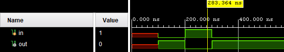
As you can see, for the first 100 nanoseconds we haven’t set the input to a value so it is floating (as indicated by red). After 100ns, we set the input to 0 and observe that the output is 1, which is what we expect for an inversion. After another 100ns, we set the input to 1 and the output becomes 0. The inverter works as expected!
Those are the basics! For information on more advanced Verilog topics, this website is a particularly useful resource: https://documentation-rp-test.readthedocs.io/en/latest/index.html